Welcome to Shenzhen Haihe Electronics Co.,Ltd
Reliable EMS Manufacturer


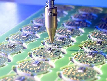
OEM/ODM capability,including circuit block program design ,PCB layout,Software program,PCBA prototype,PCBA test,SMT and DIP production S...
Read More...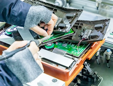
From design to market,Haihe has strong capability to make production,we have 4 SMT line,6 DIP line, 800 workers,60 engineers,20QC...
Read More...
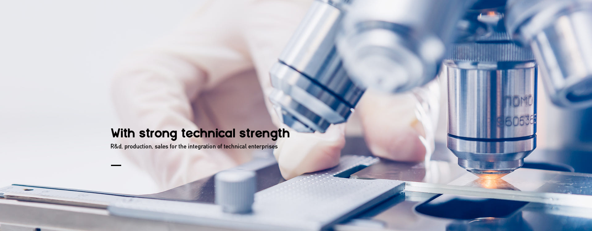
Electronic Product Industrial Design (ID) is a key factor in the commercial success of a product and every product design should start with research; who ...
Read More...
Quality is the foundation of our business, with our dedication to providing the highest quality products. Our policy is to meet or exceed our customer‘s exp...
Read More...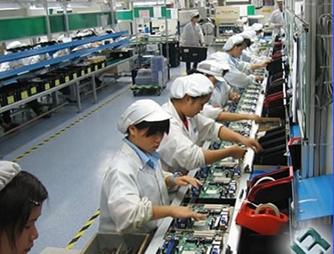
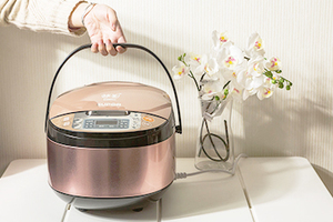
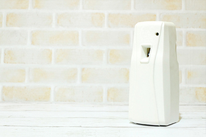
We supply turnkey service for EMS,including assembly
Read More...
We have built and sustained great relationships with all our critical suppliers, including IC and PCB suppliers. This ensures the best pricing and deliv...
Read More...


 |
+86 755 23769174 |
 |
King@odmelectronics.com |
 |
NO.10 Building,Fumin industry park,Pinghu town,Longgang district,Shenzhen, R.P.China |